SK hynix’s $13 billion HBM packaging gamble: Why building the world’s biggest memory campus matters more than you think.
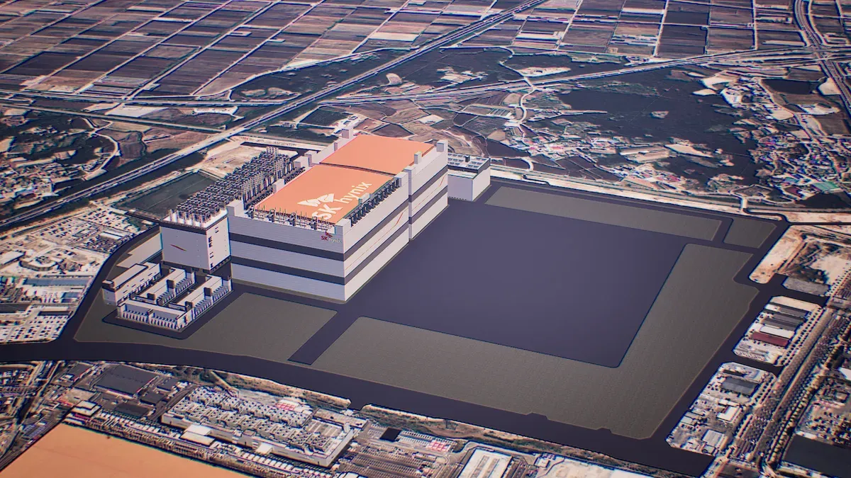
SK hynix has approved a ₩19 trillion ($13 billion) investment to construct P&T7, the world’s largest HBM packaging and testing facility in Cheongju, South Korea. The 231,405-square-meter campus will begin operations in 2027 and will focus on HBM4E, HBM5, and HBM5E production.
By situating P&T7 adjacent to its Fab M15X, SK hynix is creating a vertically integrated HBM manufacturing hub—a stark contrast to TSMC’s foundry-centric model and Intel’s Ocotillo Campus, which prioritize external partnerships over internal control.
Advanced HBM packaging now demands hybrid bonding, sub-10nm lithography, and thermal management solutions that rival the costs of 2010–2015 logic fabs. According to Anton Shilov’s analysis, TSV resistance and MR-MUF underfill complexities are driving packaging expenses to unprecedented levels.
This shift reflects the industry’s pivot from mass production to precision engineering, where yield optimization and interface tolerances for 2,048-bit HBM4+ variants are critical to profitability.
SK hynix expects HBM demand to grow at a 33% CAGR through 2030, fueled by AI accelerators and multi-chip packaging demands. The Cheongju site was chosen for its proximity to existing fabs and supply-chain resilience, not cost efficiency.
This strategic decision positions SK hynix to meet AI hardware scaling needs while maintaining control over production bottlenecks—a calculated response to the rising complexity of AI memory systems.